《Published: 23 May 2025》
Yixuan Zhao, Junhao Liao, Saiyu Bu, Zhaoning Hu, Jingyi Hu, Qi Lu, Mingpeng Shang, Bingbing Guo, Ge Chen, Qian Zhao, Kaicheng Jia, Guorui Wang, Ethan Errington, Qin Xie, Yanfeng Zhang, Miao Guo, Boyang Mao, Li Lin & Zhongfan Liu
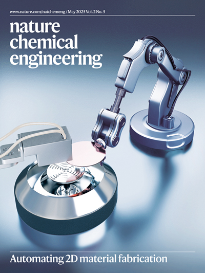
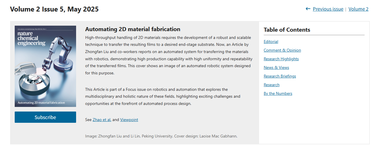
The cover of this issue of Nature Chemical Engineering features an article by Academician Liu Zhongfan and Researcher Lin Li from Peking University, and Professor Mao Boyang from the University of Cambridge, titled ‘Automated processing and transfer of two-dimensional materials with robotics.’
Research Background
In the era of rapid technological advancement, two-dimensional (2D) materials have demonstrated immense potential for next-generation electronic and photonic devices due to their unique physical and chemical properties, such as superior electrical and optical characteristics. Chemical vapor deposition (CVD) has emerged as an effective synthesis method for producing high-quality 2D materials and their heterostructures, enabling their large-scale applications. However, a critical challenge in integrating CVD-grown 2D materials into practical devices lies in their efficient and reliable transfer from growth substrates to target substrates. Currently, the lack of a scalable and stable transfer technology severely hinders the post-processing and application of CVD-synthesized 2D materials, limiting their further development in electronic and photonic devices.
Research Significance
This study successfully developed a robotic automated transfer system that achieves the automated transfer of CVD-grown 2D materials through ingeniously engineered interfacial adhesion and strain. This breakthrough holds significant implications in multiple aspects.
From an industrial application perspective, the automated transfer system exhibits high industrial compatibility. In today's industrial environment, which prioritizes efficiency and large-scale production, the system's production capacity is a key metric of its value. Remarkably, this system can process up to 180 wafers per day, far surpassing the efficiency of traditional manual transfer methods. This capability meets the industrial demand for large-scale material transfer, laying the foundation for the widespread application of 2D materials in industrial settings.
In terms of transfer quality, the system demonstrates exceptional performance. The transferred graphene exhibits a carrier mobility exceeding 14,000 cm² V⁻¹ s⁻¹, a metric that reflects the material's electrical properties post-transfer. High carrier mobility indicates superior electron transport performance, which is crucial for enhancing the functionality of electronic devices. This result confirms that the automated transfer system preserves the exceptional properties of 2D materials during the transfer process, ensuring their suitability for high-performance electronic and photonic devices.
Research Outlook
The successful development of this automated transfer system opens new opportunities and prospects for the research and commercialization of 2D materials. In the future, this system is expected to advance 2D materials in multiple dimensions.
In the research domain, the system will provide scientists with a more convenient and efficient means of material transfer, allowing them to focus more on the performance study and application development of 2D materials. Researchers can leverage this system to transfer 2D materials rapidly and accurately, facilitating various experiments and investigations to delve deeper into their physical and chemical properties, thereby providing robust support for fundamental research.
For commercialization, the system's high production capacity, reliable quality, and cost-effectiveness will drive the large-scale production and application of 2D materials. As the potential applications of 2D materials in electronics, photonics, energy, and other fields continue to expand, market demand for these materials is growing rapidly. This automated transfer system can meet the demand for large-scale, high-quality 2D materials, reduce production costs, and enhance efficiency, thereby accelerating their commercialization. It is anticipated that in the future, this system will be widely adopted in 2D material production lines, fostering rapid advancements across various industries and contributing significantly to technological progress.
Cover design process
Anhui Province Academy of Science and Technology, No. 128,Wanshui Road, Hi-Tech Zone, Hefei City, Anhui Province, China
 +86 17354022649
 service@sondii.com


 IPv6 network supported
Our hours
Beijing time: 9:00-18:00