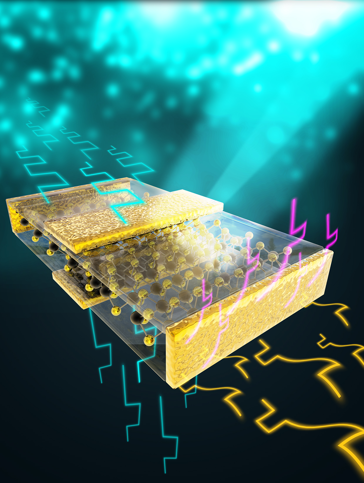
Title: Small footprint transistor architecture for photoswitching logic and in situ memory
Abstract: The need for continuous size downscaling of silicon transistors is driving the industrial development of strategies to enable further footprint reduction. The atomic thickness of two-dimensional materials allows the potential realization of high-area-efficiency transistor architectures. However, until now, the design of devices composed of two-dimensional materials has mimicked the basic architecture of silicon circuits. Here, we report a transistor based on a two-dimensional material that can realize photoswitching logic (OR, AND) computing in a single cell. Unlike the conventional transistor working mechanism, the two-dimensional material logic transistor has two surface channels. Furthermore, the material thickness can change the logic behaviour—the architecture can be flexibly expanded to achieve in situ memory such as logic computing and data storage convergence in the same device. These devices are potentially promising candidates for the construction of new chips that can perform computing and storage with high area-efficiency and unique functions.